


ACL Digital
October 14, 2024
10 Minutes read
How Can ASIC Design Services Transform Your Product Development?
Application-Specific Integrated Circuits (ASICs) are highly specialized semiconductor devices designed for a specific use case or application, offering tailored functionality and performance. Unlike general-purpose chips, which cater to a broad range of tasks, ASICs are engineered with a focused purpose, allowing for optimized performance, power efficiency, and cost-effectiveness in areas such as telecommunications, automotive, consumer electronics, and data centers. Their ability to integrate numerous functions into a single chip makes them crucial for modern electronics, especially in applications demanding low power consumption, high-speed processing, and miniaturized form factors.
ASICs play a pivotal role in an era where custom hardware is critical to differentiating products and improving efficiency. By leveraging a custom-designed chip, companies can enhance product performance while reducing power consumption and manufacturing costs. This blog serves as a comprehensive guide to the intricate process of ASIC design and development, walking through each phase, from concept to production, and exploring the engineering services that can help bring a successful ASIC project to life.
ASIC Design Process Overview
The foundation of any ASIC (Application-Specific Integrated Circuit) project begins with a critical phase: conceptualization and requirement gathering. During this stage, engineers engage with stakeholders to thoroughly understand the functional requirements, performance benchmarks, and system constraints specific to the application. This phase goes beyond high-level goals, delving into precise technical requirements like power consumption, operating frequency, and integration with other system components. The success of the ASIC project largely depends on the clarity and precision of the information gathered here, as any ambiguity could lead to costly design iterations later in the process.
Once the requirements are crystallized, the next step is the specification and design architecture. This is where the high-level functional and performance needs are transformed into a detailed design blueprint. The specification document acts as a technical guideline, describing the key building blocks of the ASIC—such as memory, I/O interfaces, and processing units—and how they interact. The design architecture is then drafted, outlining the hierarchy, data flow, and partitioning of the system to meet the required specifications. At this stage, trade-offs between power, performance, and area (PPA) are carefully balanced to ensure the architecture meets functional and manufacturability goals. This well-structured approach provides a solid foundation for the ASIC design, minimizing risks and optimizing the overall development lifecycle.
Key Phases in the ASIC Design Flow
The ASIC design flow is a systematic process divided into two critical stages: front-end and back-end design. Each phase plays a distinct role in transforming the concept into a fully functional, manufacturable chip.
Front-End Design in ASIC Development
Front-end design in ASIC development is where the core functionality of the circuit is defined and verified, setting the foundation for the entire chip. This phase involves multiple critical steps and methodologies to ensure the design logic performs as expected before proceeding to the physical design stage.
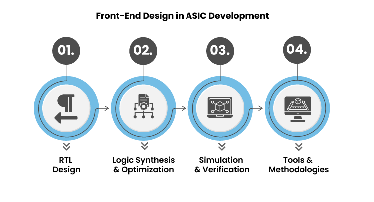
- RTL (Register Transfer Level) Design: RTL design is the cornerstone of front-end ASIC development. Engineers use hardware description languages (HDLs) like Verilog or VHDL to define the circuit’s functionality at the register level. The RTL description specifies how data moves between registers and how the circuit responds to various inputs.
- Logic Synthesis and Optimization: Logic synthesis converts the RTL code into a gate-level netlist, which is a more detailed representation of the design. Advanced optimization techniques are applied to minimize power consumption, improve speed, and optimize the area the design will occupy on the chip without compromising functionality.
- Simulation and Verification: Verification is crucial at this stage to ensure the correctness of the design. Three key types of verification are performed:
- Functional verification checks whether the design behaves as intended under different scenarios.
- Formal verification mathematically proves that the design adheres to its specification.
- Timing verification ensures that the design meets performance requirements, particularly clock timing.
- Tools and Methodologies: Advanced Electronic Design Automation (EDA) tools are vital in streamlining the front-end design process. These tools include:
- VHDL/Verilog for RTL coding and simulation
- High-Level Synthesis (HLS) abstracts design functionality and automates RTL generation from higher-level languages like C/C++, improving design productivity and efficiency.
Back-End Design in ASIC Development
In the back-end design phase of ASIC development, the logical design is translated into a physical layout that can be fabricated on silicon. This phase focuses on the physical implementation of the circuit while ensuring performance, power, and reliability. Here are the key steps involved:
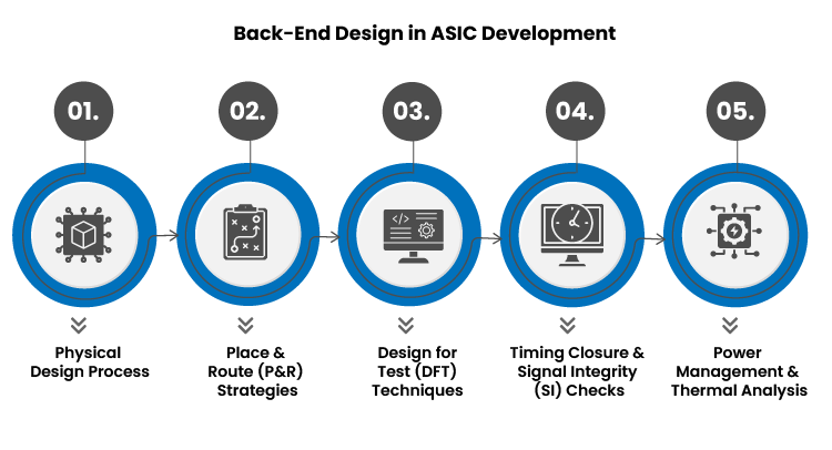
- Physical Design Process: This begins with floorplanning, where the layout of the ASIC’s key components is arranged on the chip. A well-optimized floor plan ensures that critical paths are short and allows efficient power and signal distribution. Clock tree design is also crucial at this stage, as it manages the distribution of clock signals to ensure timing consistency across all design elements.
- Place and Route (P&R) Strategies: P&R involves placing cells and routing the connections between them. Effective P&R strategies help optimize performance while minimizing wire delays and congestion. The goal is to ensure signal paths are as short as possible, reducing timing delays and ensuring a high-performance design.
- Design for Test (DFT) Techniques: DFT ensures that the ASIC can be effectively tested after manufacturing. Techniques such as scan chains, built-in self-test (BIST), and boundary scans are incorporated into the design to detect manufacturing defects and verify correct functionality in the final product.
- Timing Closure and Signal Integrity (SI) Checks: Ensuring the design meets timing constraints is critical. Timing closure involves analyzing signal propagation delays to verify that signals arrive at their destinations within the required time windows. Signal integrity checks focus on avoiding issues such as crosstalk, noise, and delay variations, which can affect the overall performance of the ASIC.
- Power Management and Thermal Analysis: Power management strategies are integrated to minimize power consumption, which is crucial in applications like mobile devices. Techniques such as power gating and dynamic voltage scaling optimize power usage. Additionally, thermal analysis ensures that heat dissipation is effectively managed, preventing overheating and ensuring reliable long-term operation of the ASIC.
Key Challenges in ASIC Design and How to Overcome Them
Designing an ASIC involves unique technical challenges requiring innovative solutions to ensure functionality and manufacturability. Here’s a breakdown of the primary challenges and how they can be effectively addressed:
- Managing Design Complexity and Integration: As ASICs grow more sophisticated, integrating millions (or even billions) of transistors on a single chip becomes increasingly complex. Engineers must handle diverse functionalities, such as signal processing, memory management, and interface integration. To overcome this, modular design techniques with IP reuse can simplify integration while maintaining design efficiency.
- Time-to-Market Pressures: In the fast-paced electronics industry, reducing design cycles while meeting deadlines is crucial. Time-to-market challenges can be mitigated through automated design workflows, leveraging advanced Electronic Design Automation (EDA) tools, and using pre-verified IP cores. This approach accelerates design processes and minimizes errors, shortening the development timeline.
- Power Consumption, Heat Dissipation, and Performance Optimization: Balancing performance with low power consumption and efficient heat dissipation is a critical challenge, especially in high-performance applications. Techniques like power gating, clock gating, and dynamic voltage scaling help reduce power consumption. Additionally, thermal-aware design practices and efficient floorplanning are essential for managing heat dissipation without compromising performance.
- ASIC Verification Complexities: Verifying an ASIC’s functionality is a demanding task that spans functional, formal, and post-silicon stages. Functional verification ensures that the design meets its intended behavior, while formal verification checks the design against its mathematical specifications. Post-silicon validation, performed after fabrication, ensures the physical chip works correctly in real-world conditions. A combination of simulation, emulation, and prototyping tools can streamline the verification process.
- Tools and Frameworks to Mitigate Challenges: Advanced EDA tools, such as Synopsys, Cadence, and Mentor Graphics, play a key role in addressing these challenges. Automated design checks, power analysis frameworks, and machine learning-driven optimization tools are essential for improving accuracy, reducing iteration cycles, and enhancing design robustness.
Why Choose ASIC Over FPGA or SoC?
- To truly understand the value of ASIC, it’s essential to compare them to other common types of integrated circuits, such as FPGAs (Field Programmable Gate Arrays) and SoCs (System on Chip). Here’s a comparative breakdown:
| Feature | ASIC | FPGA | SoC |
| Customization | Fully customized for a specific task | Programmable after manufacturing | Integrates multiple functions, including processors and peripherals |
| Performance | High performance for the designed task | Moderate performance, depending on programming | High performance across a variety of tasks |
| Power Consumption | Very low due to optimized design | Higher power consumption | Typically optimized for power efficiency |
| Flexibility | Fixed function; not reconfigurable | Reprogrammable to adapt to different tasks | Combines flexibility with integrated functionality |
| Cost | High initial development cost but cheaper for mass production | Lower upfront cost but higher per-unit cost due to flexibility | Higher development cost, similar to ASIC but integrates more functionality |
| Time to Market | Longer development time | Shorter time due to reprogrammability | Moderate time depending on complexity |
Key Factors When Choosing ASIC Design Partners
When selecting an ASIC design partner, it’s essential to look for key factors such as deep technical expertise, a proven track record in silicon engineering, and strong industry partnerships. ASIC design and development require not just cutting-edge tools but a comprehensive approach that spans from initial concept to full production. A partner with end-to-end design expertise ensures seamless integration at every stage—from specification and RTL design to physical design, verification, and final tapeout. This holistic approach minimizes risks, speeds up development cycles, and ensures high-quality outcomes.
ACL Digital is an ideal partner for ASIC design and semiconductor development. Our vast experience in silicon engineering, combined with strong partnerships with semiconductor giants like ARM, NXP, and Texas Instruments, equips us to deliver complex, high-performance ASIC solutions. We offer a full range of engineering services that significantly accelerate time-to-market, mitigate design risks, and ensure your product meets stringent technical and manufacturing standards. By leveraging our expertise and collaborative approach, clients can achieve optimal results and successfully navigate the challenges of ASIC development.
To learn more about our experience with ASIC solutions, connect with us.
Related Insights


The Rise of the Bilingual Programmer: Why “Hybrid” is the New Standard
Anagha Arun Gumaste

When NOT to use Gen AI: Architectural Boundaries and Client Expectations
Darshini Anandakumar Subha