


ACL Digital
February 21, 2025
5 Minutes read
Understanding SoC Development: From Concept to Tapeout
In today’s rapidly evolving tech landscape, System on Chip (SoC) stands at the forefront of modern electronics, driving innovation in smartphones, IoT devices, automotive systems, and more. SoC integrates multiple components—CPU, GPU, memory, and I/O controllers—onto a single chip, significantly advancing the capabilities of embedded systems. This compact design streamlines data processing minimizes physical space, and reduces power consumption, making SoCs essential for creating smarter, faster, and more efficient devices.
The shift from traditional multi-chip solutions to SoCs marks a pivotal change in electronics design. SoCs provide superior performance, lower latency, and improved energy efficiency by consolidating functions once spread across multiple chips into a single unit. This technological leap supports the growing demands for high-performance and low-power devices and paves the way for further innovations in AI, autonomous vehicles, and connected smart ecosystems.
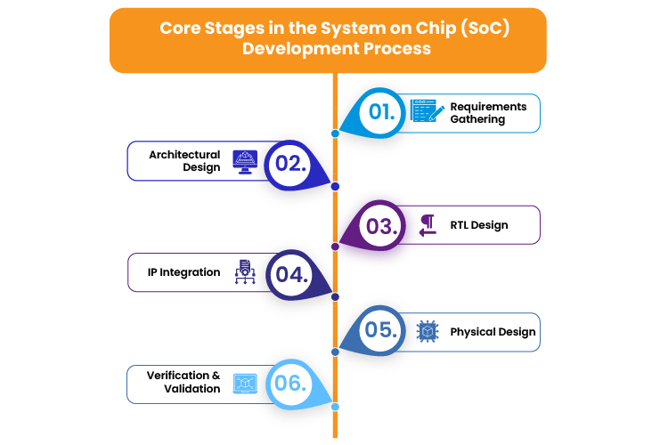
Core Stages in the System on Chip (SoC) Development Process
Developing a System on Chip (SoC) is a highly intricate process that involves multiple stages, each demanding precise attention to detail and engineering expertise. Here’s a breakdown of the key steps involved:
- Requirements Gathering: Defining system-level specifications such as performance, power, area, and cost is critical to aligning the SoC design with its intended application, whether for mobile devices, automotive systems, or industrial equipment. Understanding the application-specific needs ensures the SoC is optimized for its target use case.
- Architectural Design: High-level architecture planning involves partitioning the design and selecting the appropriate IP (Intellectual Property) blocks. Key decisions must balance trade-offs between performance, power efficiency, and die size to meet overall system goals.
- RTL (Register Transfer Level) Design: The RTL design phase uses hardware description languages like Verilog or VHDL to define the functional behaviour of the chip. This phase also includes functional simulation and verification to ensure the design meets the desired functionality before moving forward.
- IP Integration: Integrating third-party IP cores or in-house developed IP is critical. This involves ensuring compatibility and interoperability across different blocks within the SoC, which can significantly affect both performance and system integration.
- Physical Design: Floorplanning, placement, and routing are central to the physical design phase. Power, thermal, and signal integrity management are carefully handled to optimize the chip’s real-world performance. DRC (Design Rule Checking) and LVS (Layout vs. Schematic) are also performed to ensure manufacturing accuracy.
- Verification and Validation: SoC verification involves multiple methods, including simulation-based verification, emulation, and formal verification. Using FPGA prototyping, hardware simulation, and other techniques, system-level validation ensures the design works as intended in actual hardware environments.
Each stage in the SoC development process requires a seamless integration of tools, techniques, and engineering understanding to ensure that the final product meets stringent performance, power, and design standards.
Key Challenges in Modern SoC Design
- Increasing Design Complexity: As SoC designs evolve, managing the growing number of transistors and integrating various IP (Intellectual Property) blocks becomes a significant challenge. With billions of transistors packed into a single chip, they ensure optimal performance while minimizing errors, demanding advanced design tools and methodologies. Moreover, verifying these complex systems is critical to avoid functional flaws, but it often results in time-to-market pressures. Meeting these challenges requires sophisticated verification frameworks and automation tools capable of handling the complexity of modern SoC designs.
- Power and Thermal Management: High-performance SoCs must handle significant thermal constraints, especially in demanding applications like automotive or AI processors. Efficient power management becomes a delicate balancing act between performance and energy efficiency, particularly in devices like IoT sensors, where low power is crucial for extended battery life. In contrast, high-end computing devices prioritize performance, often pushing power and thermal limits. Advanced techniques like dynamic voltage scaling, clock gating, and thermal management algorithms ensure that SoCs operate optimally across various use cases.
- Time-to-Market Constraints: Accelerating the SoC development cycle while maintaining high quality is a constant challenge for manufacturers. Given the competitive landscape, delays in design or verification can significantly impact a product’s market success. Streamlining the verification and validation processes through simulation, emulation, and advanced design automation tools is essential. Additionally, leveraging pre-verified IP blocks and adopting agile development methodologies helps reduce development times without compromising the performance or reliability of the final product.
The Advanced Strategies in SoC Design
Let’s explore advanced strategies in SoC design, including hardware-software co-design for performance optimization, Design for Manufacturability (DFM) to ensure yield at smaller process nodes, and the integration of AI/ML accelerators, along with AI-driven automation tools that streamline the SoC development process.
- Hardware-Software Co-design: To optimize SoC performance, hardware-software co-design ensures that both components are developed in tandem. This approach balances the hardware’s processing power with the software’s efficiency, reducing bottlenecks and improving overall system performance. High-level synthesis (HLS) tools are crucial in converting software algorithms into hardware code, allowing for rapid prototyping and faster time-to-market.
- Design for Manufacturability (DFM): As process nodes continue to shrink (7nm, 5nm, etc.), ensuring that SoCs are optimized for manufacturability is critical. DFM techniques minimise manufacturing variations and defects, which can compromise yield at smaller geometries. Yield optimization strategies include layout enhancements, process variability management, and defect tolerance to maximize chip production efficiency without compromising performance.
- AI/ML in SoC Design: Machine learning accelerators like TPUs (Tensor Processing Units) and NPUs (Neural Processing Units) are increasingly integrated into SoC architectures to support AI-driven applications. These accelerators handle specialized tasks like neural network inference, offering higher computational efficiency. Additionally, AI-driven design automation tools are transforming SoC development by automating layout optimization and verification processes, reducing design time while enhancing accuracy.
Verification and Testing in SoC Development
Verification and testing are pivotal in SoC development, ensuring the design meets functional and performance specifications. The following vital processes drive these stages:
- Functional Verification: This phase ensures the SoC operates correctly before fabrication. Pre-silicon simulations leverage coverage-driven methodologies to verify the logic across various scenarios. Universal Verification Methodology (UVM) is widely used to build reusable test benches, enabling thorough testing of individual IP blocks and the complete SoC design.
- Physical Verification: After layout completion, physical verification ensures the design conforms to manufacturing constraints and meets operational stability requirements. Key processes include Design Rule Checking (DRC) and Layout vs. Schematic (LVS) to ensure the layout matches the schematic. Timing analysis identifies signal path delays, while power analysis evaluates energy efficiency. Thermal analysis and signal integrity checks confirm the design’s stability under varying temperature and noise conditions.
- Manufacturing and Post-Silicon Validation: Once fabricated, silicon bring-up powers the first chip to validate functionality. Test vectors are applied to confirm performance, while debugging techniques identify any issues. Design for Testability (DFT) features, such as built-in self-test (BIST), facilitate efficient troubleshooting and ensure the SoC operates reliably in real-world environments.
Advanced EDA Tools for Streamlined SoC Design and Verification
In the complex landscape of SoC development, specialized Electronic Design Automation (EDA) tools are pivotal in streamlining the design, simulation, and verification processes. Synopsys Design Compiler and Cadence Encounter are widely used for front-end design tasks such as synthesis, RTL (Register Transfer Level) implementation, and initial validation. These tools convert high-level hardware descriptions into gate-level netlists, ensuring the design meets performance, area, and power constraints. For back-end tasks, tools such as Mentor Graphics Calibre are essential for physical verification, ensuring that the layout adheres to manufacturing rules and seamless chip-level integration.
Simulation tools like Mentor Questa and Cadence Xcelium also provide high-fidelity functional verification, allowing developers to test SoC behaviour rigorously before manufacturing. Design and simulation are often accompanied by FPGA prototyping tools, such as Xilinx Vivado, enabling early hardware validation and system-level testing. These tools, paired with AI-driven optimizations in the latest EDA suites, accelerate the entire development cycle, from design conception to final tape-out, ensuring robust and efficient SoC implementations across industries.
How Does ACL Digital Empower Semiconductor Companies in SoC Design and Development?
ACL Digital has extensive experience supporting chip manufacturers and semiconductor companies in designing and developing advanced SoCs tailored to meet specific industry requirements. Our expertise spans the semiconductor lifecycle, from concept and architecture design to verification, physical design, and post-silicon validation. Leveraging cutting-edge EDA tools and deep knowledge of advanced process nodes, we ensure optimized power, performance, and area (PPA) for next-generation SoCs.
Our capabilities include custom IP development, integration of multi-core processors, memory subsystems, and high-speed peripheral interfaces, all while addressing challenges like power efficiency and thermal management. With proven partnerships across leading semiconductor players, ACL Digital’s engineering services enable faster time-to-market, seamless hardware-software integration, and highly scalable SoC solutions for industries ranging from automotive to consumer electronics and telecommunications. Our SoC expertise empowers clients to innovate rapidly while overcoming the complexities of modern semiconductor design.
For more information about our comprehensive semiconductor engineering capabilities, please contact us at business@acldigital.com.