

ACL Digital
August 20, 2024
7 Minutes read
The Wafer Fabrication Process is the Heart of Semiconductor Manufacturing
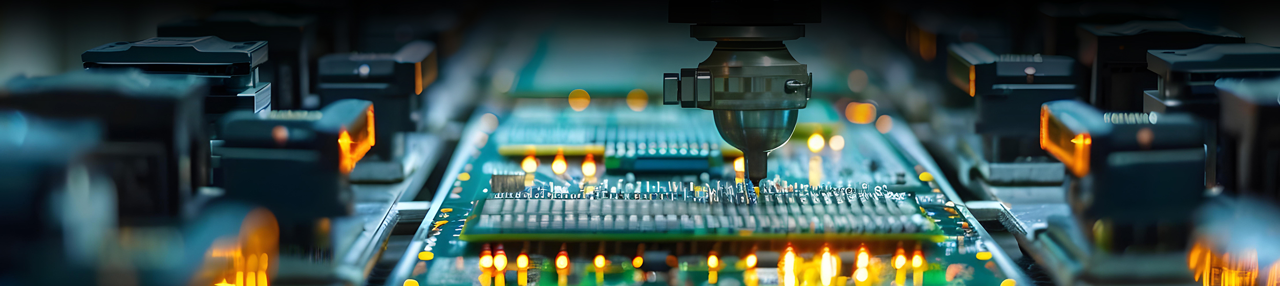
The semiconductor industry is a cornerstone of modern technology, powering everything from smartphones to supercomputers. At the heart of this industry lies the wafer fabrication process, a sophisticated series of steps that transform raw silicon into the semiconductor wafers that drive our electronic devices. The article delves into the intricacies of wafer fabrication, providing an in-depth look at the process, the materials used, and the latest advancements.
What is Wafer Fabrication?
Wafer fabrication creates semiconductor wafers, thin slices of semiconductor material, typically silicon, used to produce integrated circuits (ICs). This complex process involves multiple stages, including wafer manufacturing, wafer processing, and the integration of circuits onto the wafer. The result is an integrated circuit wafer ready for assembly into electronic devices.
The Importance of Semiconductor Wafers
Semiconductor wafers are the building blocks of the electronic world. They are the substrate upon which various electronic components, such as transistors, resistors, and capacitors, are fabricated. The quality and precision of these wafers directly impact the final electronic products’ performance, reliability, and efficiency.

Semiconductor wafers are created from highly purified single crystals. While silicon is the most common material, a variety of other substances are also employed:
- Germanium
- Gallium arsenide (GaAs)
- Silicon carbide (SiC)
- Indium phosphide (InP)
- Silicon germanium (SiGe)
- Sapphire (Al2O3)
- Gallium nitride (GaN)
- Zinc oxide (ZnO)
- Diamond
Key Drivers of Silicon Wafer Demand
Several factors are boosting demand for silicon wafers in the U.S.:
1. Increased Use of Semiconductors
Semiconductors are now crucial components in a wide range of products, including cars, communication networks, and smart devices. As more semiconductors are used in each product, the demand for silicon wafers to produce semiconductors increases. We anticipate continuing this trend, leading to double-digit demand growth for our silicon wafers until at least 2025.
2. Technological Advancements
Ongoing technological advancements in computing, communications, automotive technology, and the Internet of Things (IoT) drive demand for more advanced and larger silicon wafers. These new technologies require more sophisticated chips, increasing the need for higher-quality wafers.
3. The Materials: Silicon Wafer Material
Silicon is the predominant material used in wafer fabrication due to its excellent electrical properties and abundance in nature. Semiconductor silicon wafers are made from highly pure silicon crystals. These crystals are grown using the Czochralski process, where a seed crystal is dipped into molten silicon and slowly pulled out while rotating. This process forms a cylindrical silicon ingot, which is then sliced into thin wafers.
Wafer Manufacturing: From Ingot to Wafer
The journey from silicon ingot to semiconductor wafer involves several critical steps:
Ingot Growth
As mentioned, the Czochralski process grows large, single-crystal silicon ingots. This step is crucial for ensuring the purity and uniformity of the silicon wafer material.
Slicing
A diamond saw cuts the silicon ingot into thin, circular slices called wafers. These wafers are typically 200mm to 300mm in diameter, with the thickness varying depending on the application.
Polishing
After slicing, the wafers are polished to achieve a mirror-like surface. This step is essential for the subsequent photolithography process, in which intricate circuit patterns are etched onto the wafer.
Cleaning
The polished wafers undergo a thorough cleaning to eliminate any contaminants. Even tiny particles can impact the performance of the finished integrated circuit wafer.
Wafer Processing: Creating the Integrated Circuits
Once the silicon wafers are prepared, they undergo a series of wafer processing steps to create the integrated circuits:
Photolithography
This process starts by coating the wafer with a light-sensitive material called photoresist. Next, a mask with the desired circuit pattern is placed over the wafer, and ultraviolet light transfers the pattern onto the photoresist. The exposed areas are then developed, revealing the circuit design.
Etching
Chemical or plasma etching removes unwanted silicon, leaving intricate circuit patterns behind. This process is repeated several times to create the layered structure of the integrated circuit.
Doping
Doping introduces impurities into specific areas of the silicon wafer to alter its electrical properties. It is usually done via ion diffusion and implantation methods.
Deposition
Thin layers of materials, such as metals and insulators, are deposited onto the wafer to create the components of the integrated circuit. Common techniques for material deposition include chemical vapor deposition (CVD) and physical vapor deposition (PVD).Planarization
This phase ensures uniformity across all layers by smoothing the wafer’s surface. Chemical mechanical planarization (CMP) is a typically used technique.Testing and Inspection
Throughout the wafer fabrication steps, rigorous testing and inspection are conducted to ensure the wafers’ quality and functionality. Advanced metrology tools and techniques detect any defects or irregularities.
Recent Advancements in Wafer Fabrication
The semiconductor industry continually evolves, with new technologies and methods enhancing the wafer fabrication process. Some of the latest advancements include:
Extreme Ultraviolet Lithography (EUVL)
EUVL enables the creation of smaller and more precise circuit patterns, producing advanced chips with higher performance and lower power consumption.
3D Integration
This technology stacks multiple circuit layers vertically, enhancing the density and functionality of semiconductor devices. 3D integration is especially advantageous for high-performance applications and compact form factors.
Gallium Nitride (GaN) Wafers
While silicon remains the dominant material, GaN wafers are gaining traction due to their superior electrical properties, especially for high-frequency and high-power applications.
Quantum Computing
The development of quantum computing is driving innovations in wafer fabrication, with new materials and processes being explored to create qubits and quantum circuits.
The Business Perspective: Why Wafer Fabrication Matters
From a business standpoint, wafer fabrication is a critical component of the semiconductor supply chain. The efficiency, cost, and quality of the wafer fabrication process directly impact semiconductor companies’ competitiveness. As the demand for advanced electronic devices continues to grow, companies that can innovate and optimize their wafer fabrication processes will have a significant advantage in the market.
Investments in cutting-edge wafer fabrication technologies, such as EUVL and 3D integration, can lead to chip performance and efficiency breakthroughs. Additionally, wafer manufacturing and processing advancements can reduce production costs, increase yield, and improve time-to-market for new products.
Conclusion
Wafer fabrication is a fascinating and intricate process underpinning the semiconductor industry. Each step requires precision, innovation, and expertise, from the raw silicon ingot to the polished, intricate integrated circuit wafer. Wafer fabrication will continue to be essential in creating the advanced electronics of the future. It will drive new technologies and help develop more innovative, efficient devices.
For semiconductor businesses, staying at the forefront of wafer fabrication technology is essential. Companies can ensure their place in the rapidly evolving tech landscape by understanding the process, investing in the latest advancements, and continually optimizing production.
References
About the Author
ACL Digital
Related Insights

Latest Technological Developments in Embedded and Semiconductor Industry
ACL Digital
October 26, 2021

The Contribution of Semiconductors to the Automotive Industry
ACL Digital
April 25, 2022

Essential Things You Should Know About FPGA Security
ACL Digital
November 14, 2022

The Top Semiconductor Innovations and Trends in 2023
ACL Digital
February 1, 2023