


ACL Digital
February 21, 2025
5 Minutes read
Revolutionizing VLSI Engineering with AI-Driven Physical Design Optimization
The convergence of Very Large Scale Integration (VLSI) engineering and artificial intelligence (AI) is revolutionizing the semiconductor industry, addressing some of its most complex challenges. VLSI engineering, the backbone of modern chip design, underpins the creation of advanced, high-performance integrated circuits powering everything from smartphones to autonomous vehicles. However, as design complexity escalates with shrinking nodes and increasing transistor densities, traditional methodologies often fail to meet performance, power efficiency, and time-to-market demands.
AI steps in as a transformative force. By automating and optimizing critical aspects of physical design such as floorplanning, placement, and routing, AI enhances efficiency and precision in ways previously unattainable. Its capabilities extend to predicting design outcomes, optimizing power consumption, and ensuring compliance with stringent design rules, all while accelerating timelines. As the semiconductor industry faces mounting pressure for faster innovation cycles, AI-driven physical design optimization is emerging as a vital enabler for achieving next-generation chip performance and reliability.
Key Challenges in Physical Design Optimization for VLSI Engineering
Physical design optimization in VLSI engineering is a critical phase in chip design, transforming logical designs into manufacturable layouts. However, the demand for higher performance, lower power consumption, and smaller form factors introduces complex challenges, particularly at advanced process nodes like 3nm and 2nm. Key challenges include:
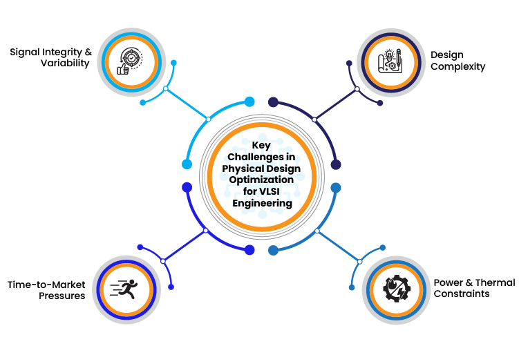
- Design Complexity: The exponential increase in transistor density pushes design boundaries to accommodate billions of components on a single chip. Advanced process nodes require precise placement and routing strategies, accounting for tighter design rules, reduced feature sizes, and increased interconnect density. Achieving optimal performance without compromising manufacturability becomes increasingly intricate.
- Power and Thermal Constraints: The dual goals of high performance and energy efficiency are often at odds, especially in applications ranging from IoT devices to high-performance computing. Designers must address power leakage, optimize dynamic power consumption, and ensure thermal stability. Techniques like clock gating and multi-voltage domains require careful implementation to manage these constraints effectively.
- Time-to-Market Pressures: The semiconductor industry’s competitive landscape demands shorter development cycles without compromising quality. Accelerating design timelines while adhering to stringent performance and reliability benchmarks often requires advanced automation tools to streamline processes like floorplanning, routing, and verification.
- Signal Integrity and Variability: Managing signal integrity is crucial to maintaining chip reliability, as issues like crosstalk, electromagnetic interference, and timing delays can jeopardize performance. Additionally, process variations at nanoscale geometries lead to unpredictable behavior, requiring robust statistical models and adaptive design techniques to mitigate their impact on yield and functionality.
Role of AI in Physical Design Optimization
AI has become a game-changer in VLSI engineering, addressing challenges of scale, complexity, and efficiency with unmatched precision. Leveraging advanced algorithms and data-driven insights, AI revolutionizes critical aspects of the design workflow:
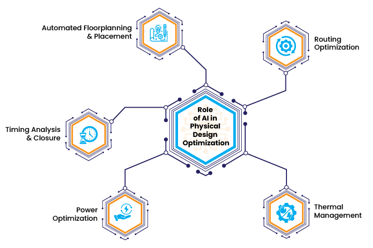
- Automated Floorplanning and Placement: AI algorithms analyze design constraints and objectives to predict optimal chip layouts. This ensures a balanced trade-off between power, performance, and area (PPA), significantly reducing the iterative manual adjustments traditionally required. AI-driven floorplanning adapts to varying workloads, delivering dynamic solutions tailored to specific design needs.
- Routing Optimization: AI-powered tools resolve routing congestion by predicting potential bottlenecks and optimizing signal paths. Advanced models ensure signal integrity and minimal crosstalk, even in highly complex designs where traditional algorithms struggle with scalability.
- Thermal Management: Machine learning models simulate thermal profiles to predict hotspots and recommend efficient heat dissipation paths. By integrating thermal awareness into the design phase, AI minimizes temperature-induced reliability issues, which is especially critical for high-performance and low-power designs.
- Power Optimization: AI identifies and mitigates power leakage while optimizing dynamic power consumption. AI enables techniques like dynamic voltage scaling and clock gating for energy-efficient designs that meet stringent power constraints without compromising performance.
- Timing Analysis and Closure: AI accelerates timing convergence by predicting critical path delays and automating design adjustments. This results in faster validation cycles, ensuring designs meet performance targets, even at advanced nodes like 5nm and beyond.
Emerging Trends in AI-Driven VLSI Physical Design
The intersection of AI and VLSI engineering is revolutionizing physical design processes, bringing unprecedented efficiency, accuracy, and scalability. Here are the most impactful trends reshaping this landscape:
- Reinforcement Learning (RL) in Design Automation: Reinforcement Learning (RL) is emerging as a game-changer in automating placement and routing tasks. By training agents to make optimal decisions in complex design scenarios, RL enables dynamic exploration of power, performance, and area (PPA) optimization solutions. Advanced techniques like policy gradients and Q-learning address intricate trade-offs, significantly reducing design cycle times.
- AI-Assisted Design for Manufacturability (DFM): AI-enhanced DFM tools maximize manufacturability while mitigating potential defects. These tools enable preemptive adjustments during the design phase by predicting variations and yield issues. Machine learning models analyze process data and design layouts to improve lithography, manage variability, and enhance yield, particularly in sub-7nm nodes.
- Generative AI in Layout Synthesis: Generative AI models, leveraging techniques like Generative Adversarial Networks (GANs), are now pivotal in automating block-level and chip-level layout generation. These models accelerate layout synthesis but also ensure compliance with stringent design rules. Their adaptability proves instrumental in meeting diverse application-specific requirements.
- Integration with Advanced EDA Tools: EDA giants like Synopsys and Cadence are leading the integration of AI into design workflows. Platforms such as Synopsys DSO.ai and Cadence Cerebrus utilize AI-driven algorithms to automate synthesis, verification, and optimization tasks. These tools learn from historical projects to improve decision-making, reduce time-to-market, and achieve superior PPA.
- Collaborative AI for Multi-Objective Optimization: With global teams contributing to VLSI projects, collaborative AI models foster synchronized efforts in achieving multi-objective optimization. Distributed AI systems enable real-time data sharing and decision-making, addressing constraints such as power leakage, signal integrity, and thermal management across multiple design hierarchies.
These advancements show that AI is a tool and a transformative force in VLSI physical design, pushing the boundaries of semiconductor engineering.
Best Practices for Selecting AI Tools in VLSI
Selecting the right AI tools is critical for optimizing VLSI workflows. Here’s what engineers should prioritize:
- Ease of Integration and Interoperability: AI tools must seamlessly integrate with existing Electronic Design Automation (EDA) ecosystems like Cadence, Synopsys, or Mentor Graphics. Compatibility with widely used formats such as Verilog, VHDL, and standard design flows ensures smooth adoption without disrupting workflows.
- Scalability for Complex Design Requirements: Scalability is critical for AI tools in handling varying design complexities. From basic IP block verification to large-scale SoC (System-on-Chip) designs, the tool should adapt to projects of all sizes while maintaining performance accuracy. Scalability ensures that the tool grows with the project’s demands, optimizing performance for multi-billion transistor designs and advanced nodes like 5nm or 3nm.
- Customization for Targeted Optimization: AI tools should offer customization capabilities, such as fine-tuning machine learning models to align with specific design constraints like power, area, and timing. For instance, tools that enable custom training of AI models to identify recurring design patterns or optimize layout placement for unique architectures provide a competitive edge in achieving high-efficiency designs.
- Vendor Partnerships: It is crucial to collaborate with vendors that provide robust AI-driven EDA tools. Companies investing in AI innovation, such as Synopsys with its DSO.ai or Cadence’s Cerberus, often lead the market with cutting-edge capabilities. Strong vendor partnerships ensure consistent updates, better support, and access to industry-leading technologies tailored to advanced VLSI workflows.
Unlocking the Future of VLSI with AI-Driven Physical Design Optimization
AI’s transformative potential in physical design optimization reshapes VLSI engineering, delivering precise control over power, performance, and area metrics while significantly reducing design iterations and time-to-market. Advanced AI algorithms excel at addressing the intricate challenges of placement, routing, and timing closure, automating processes that traditionally relied on manual intervention. By integrating machine learning models, VLSI engineers can achieve predictive design adjustments, optimize resource utilization, and ensure scalability, even as semiconductor technologies advance to sub-3nm nodes. This paradigm shift is more than an efficiency booster; it is necessary to meet the rising demands of AI/ML accelerators, 5G chipsets, and IoT ecosystems.
At ACL Digital, our extensive expertise in the VLSI and semiconductor industry is driving innovation for customers across domains. Leveraging AI-enabled methodologies, we deliver tailored solutions for physical design optimization, including seamless integration of cutting-edge EDA tools and process-specific optimizations. By partnering with semiconductor leaders such as NXP, ARM, Silicon Labs, Infineon, etc, we help accelerate tape-outs, enhance design quality, and align with the latest advancements in AI-driven workflows. Contact us today to explore how AI-powered solutions can transform your VLSI design workflows and position your business for success in a competitive landscape.
Related Insights