


ACL Digital
August 22, 2024
5 Minutes read
Protect and Validate Essential JTAG Practices for Electronics
In the rapidly evolving electronics industry, ensuring the quality and functionality of electronic assemblies is paramount. One critical technology that has become indispensable for verifying designs and testing printed circuit boards (PCBs) is the Joint Test Action Group (JTAG). Established as a technical standard and transformed how engineers approach testing and debugging in the manufacturing process.
JTAG was developed in the mid-1980s by a consortium of European electronics companies to address the challenges of testing complex integrated circuits (ICs) and dense PCBs. The IEEE 1149.1 standard, established in 1990, provided a standardized method for boundary scan tests on digital circuits, allowing engineers to test connections without physical probes, which was essential for high-density boards.
JTAG Architecture
The JTAG architecture includes a Test Access Port (TAP), an Instruction Register (IR), and a Data Register (DR). The TAP serves as the interface between the JTAG controller and the test device. The DR enables data transfer between the device and the controller, while the IR holds and manages the instructions for device operation.
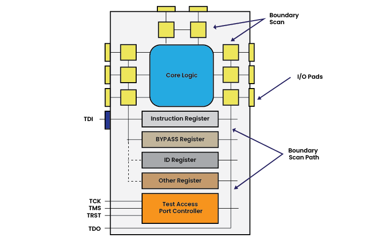
The JTAG architecture consists of several key components:
- Test Access Port (TAP): A standard interface on the device, typically comprising four or five pins (TDI, TDO, TMS, TCK, and optionally TRST).
- TDI (Test Data In): Serial input for test instructions and data.
- TCK (Test Clock): Clock signal to synchronize data shifting.
- TMS (Test Mode Select): Used to control the state machine of the test logic.
- TRST (Test Reset):Often used to reset the test logic.
- TDO (Test Data Out): Serial output for test data results.
- Instruction Register (IR): Receives the instructions from the TAP controller.
- Data Registers (DR): Hold the data related to the JTAG instructions.
- TAP Controller: Manages the operations of JTAG, operating in various states such as Test-Logic-Reset, Run-Test/Idle, and various Shift and Update states.
Design-for-Test Considerations
When designing a JTAG-testable board, several guidelines should be followed to ensure successful implementation:
- Group programmable components in the chain order and provide access to TDI and TDO signals.
- Ensure all parts in the boundary-scan chain have 1149.1-compliant TAPs.
- Use simple buffering for TCK and TMS signals to simplify test considerations.
- Group similar device families and use a single level converter interface.
- Use the standard JTAG connector as depicted in Corelis documentation.
- Ensure BSDL files are available and validated for each JTAG component used on the board.
Advantages of JTAG
JTAG offers several advantages, making it a preferred choice for testing and debugging in the electronics industry:
- JTAG tests PCBs without physical probes, minimizing damage risk to delicate components.
- JTAG provides access to internal logic for comprehensive testing of devices and board interconnections.
- JTAG supports a variety of applications, including testing, programming, and debugging.
- JTAG’s standardized interface accelerates development and testing, shortening time-to-market.
- JTAG lowers testing and manufacturing costs by reducing the need for extensive fixtures and equipment.
Challenges with JTAG
Although JTAG (Joint Test Action Group) is a valuable tool for debugging and testing electrical equipment, it is still vulnerable to security flaws. We’ll look at a few typical attacks that might jeopardize hardware security by targeting JTAG ports.
Physical Access Attacks
Physical access attacks occur when an attacker gains direct access to a device’s JTAG interface, allowing them to perform unauthorized actions, extract private data, or introduce malicious code. In direct probing, attackers use probes or connections to interact with JTAG pins, bypassing security measures to read or modify the device’s internal state. In chip-off attacks, attackers desolder the chip from a device, such as a smartphone, to access the JTAG interface and extract sensitive information.
Side-Channel Attacks
Side-channel attacks exploit unintended information leakage from physical characteristics like power usage, electromagnetic emissions, or timing variations during JTAG operations. In power analysis, attackers analyze power consumption patterns to gain insights into internal states and cryptographic keys. Timing analysis involves examining the timing of JTAG signals to deduce critical information, such as encryption keys or execution pathways. These attacks leverage subtle variations to breach device security.
Glitch Attacks
Glitch attacks manipulate the timing or voltage levels of JTAG signals to disrupt a device’s normal operation. By injecting glitches, attackers can bypass security measures or extract data. Voltage glitching involves altering voltage levels during specific JTAG operations to cause improper device behavior. Clock glitching involves changing the clock signal to induce timing errors, exploiting vulnerabilities in the JTAG controller. These techniques allow attackers to interfere with standard JTAG processes and compromise device security.
Firmware Manipulation
Attackers can exploit the JTAG interface to modify or replace a device’s firmware, installing malicious code, backdoors, or unauthorized programs. This manipulation of the JTAG port can lead to significant security risks, as it may allow attackers to compromise or take control of the device. Such vulnerabilities highlight the importance of securing JTAG interfaces to prevent unauthorized access and ensure device integrity.
How to Mitigate Challenges with JTAG?
JTAG (Joint Test Action Group) attacks can significantly threaten the security of hardware systems. Implementing effective mitigation techniques is crucial to ensure the integrity and confidentiality of sensitive information.
Protect JTAG Access
To prevent unauthorized manipulation, it is essential to limit physical access to JTAG interfaces. Use physical protection methods, such as placing JTAG connections in tamper-evident enclosures or restricted areas, to guard against physical assaults. Implement access controls by using robust authentication methods like passwords or biometric systems to ensure that only authorized individuals can access JTAG interfaces. For example, securing a JTAG interface with a biometric lock can prevent unauthorized personnel from tampering with sensitive electronic devices.
Turn Off JTAG by Default
To minimize security risks, JTAG capabilities should be disabled by default in production systems or end-user devices. This precautionary measure reduces the potential attack surface by ensuring that the JTAG interface cannot be exploited unless specifically enabled for essential testing or debugging purposes. For instance, manufacturers can implement a system where JTAG is only activated temporarily during authorized maintenance activities, thereby protecting devices from unauthorized access.
Configure JTAG Securely
To reduce the risk of unauthorized access to the JTAG controller, implement robust security measures. Enforce strong passwords for accessing the JTAG interface, ensuring that default passwords are changed during initial setup. Additionally, utilize encryption techniques to secure JTAG communications, preventing eavesdropping and manipulation. For instance, employing AES encryption can protect the data transmitted via JTAG, enhancing overall security.
Secure Boot and Firmware Validation
Secure Boot verifies the integrity and authenticity of the firmware during the boot process, ensuring that only trusted, signed firmware is executed. Digital Signatures involve using cryptographic keys to sign firmware images, with the system checking these signatures at boot to detect tampering or unauthorized alterations. For example, a firmware image signed with a private key can be verified against its public counterpart to confirm its legitimacy.
Monitoring and Threat Detection
To detect and respond to potential JTAG attacks, establish comprehensive monitoring and intrusion detection systems. Implement auditing and logging to record JTAG operations and regularly review logs for unauthorized or suspicious activities. Deploy Intrusion Detection Systems (IDS) to monitor JTAG communication and alert you to any suspicious or malicious behavior. Additionally, perform routine hardware and firmware integrity checks to identify and address any tampering or alterations.
Continuous Security Updates
Regularly update your hardware devices’ firmware by applying the latest security patches from manufacturers. These updates fix vulnerabilities and enhance security. For example, installing a firmware update that addresses a known security flaw can protect against new types of cyberattacks, ensuring your device remains secure.
Applications of JTAG
JTAG offers a wide range of applications in device testing and programming, providing engineers with powerful tools to enhance electronic products. Here are the key applications:
Debugging
JTAG is employed by engineers to inspect and modify internal registers, perform boundary scans, and monitor device signals. This capability is crucial for identifying and resolving hardware issues, streamlining development processes, and reducing associated costs.
In-System Programming (ISP)
JTAG facilitates in-system programming, allowing changes to firmware or configuration data of programmable devices like microcontrollers and FPGAs without the need for external hardware.
Boundary Scan
JTAG’s boundary scan capability allows engineers to test individual components, verify interconnections, and detect manufacturing flaws in high quality PCBs. This process is essential for ensuring the integrity of connections without the need for physical probes.
Chip Testing
During production, JTAG is extensively used to test integrated circuits, ensuring their quality and reliability before they are incorporated into finished goods.
Conclusion
Testing and debugging electronic assemblies requires the use of JTAG technology in the rapidly evolving electronics industry. From its origins to its current applications in device testing, programming, and security, JTAG has significantly advanced the way engineers address hardware challenges. While JTAG offers powerful tools for device verification, it also presents security risks that require vigilant protection. Implementing robust measures are essential for mitigating potential threats. By following best practices and keeping security protocols up to date, manufacturers and engineers can safeguard their devices against unauthorized access and maintain the integrity of their electronic systems.
For the latest updates or additional information, feel free to contact ACL Digital.
Related Insights

Beyond the Black Box: The Role of Explainable AI (XAI) in Enabling Ethical and Responsible AI Adoption
Jayshree Rathod
April 21, 2025

Why AI-Powered Marketing Is Key to Business Growth
Tharik Mohamed Alikul Jaman
April 21, 2025

How multimodal interactions enhance the experience of commerce
Balasubramanian
April 17, 2025

The Game-Changing Potential of 5G in Consumer Devices
ACL Digital
January 15, 2025

The Role of Artificial Intelligence in Shaping the Future of Consumer Electronics
ACL Digital
June 28, 2024